Casa> Blog> SMT steel mesh PCB steel mesh solder paste template development trend - SMT laser steel mesh

SMT steel mesh PCB steel mesh solder paste template development trend - SMT laser steel mesh

November 16, 2022

Pad and stencil opening for common components in SMT process

--Xin Ge Rui produces China's good SMT steel mesh (template)

The manufacturability design ( OEM ) in the SMT process is increasingly being looked at by OEMs , ODMs and EMS vendors. An optimized manufacturability design enables the product to be manufactured better, reducing the manufacturing difficulty factor and avoiding the possibility of being repaired. Not only can it be delivered faster and better, but it can also save a certain amount of specimens and create profits.

The key point in the SMT process is soldering. It can be said that SMT is the process of how to place a component in a predetermined position and achieve a certain electrical performance by soldering.

How to design a reasonable pad according to the size and characteristics of the component, how to design the stencil according to the component and the pad and solder joint requirements, and the designed pad and stencil are manufacturable, which will be faced by a process engineer. problem.

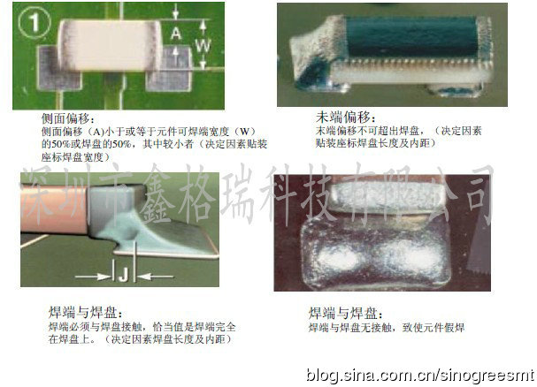
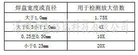
Remarks: 1. The standard involved in the document is the secondary standard in IPC-A-610 . The inspection method involved is obtained by the following magnification:

Pad and stencil opening instructions for common components in SMT process


2 , the default components in the text are standard parts, based on this design of the pad and steel mesh.

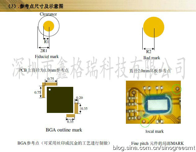
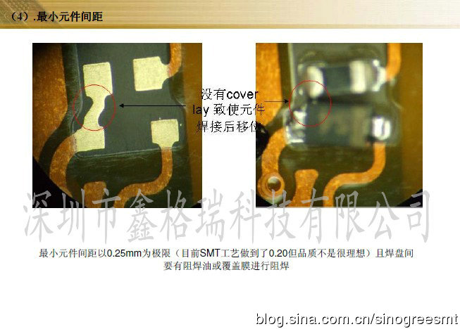
  1,          The manufacturability of the PCB .

Pad and stencil opening instructions for common components in SMT process

Pad and stencil opening instructions for common components in SMT process

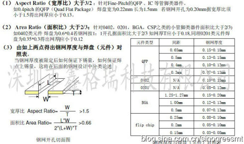
2,          The manufacturability design of the steel mesh.

In order to make the solder paste better formed after printing, the steel mesh should pay attention to the following requirements in thickness selection and opening design:

Pad and stencil opening instructions for common components in SMT process


3 , common components in the SMT process and its pad steel mesh opening design

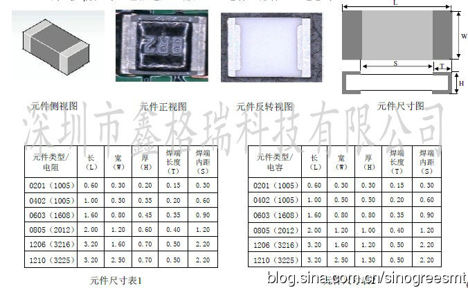
  ( 1 ) Chip component size: including resistance (exclusion), capacitance (discharge), inductance, etc.

Pad and stencil opening instructions for common components in SMT process

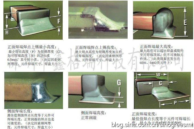
( 2 ) Soldering requirements for solder joints of chip components: including resistance (exclusion), capacitance (discharge), inductance, etc.

Pad and stencil opening instructions for common components in SMT process

Pad and stencil opening instructions for common components in SMT process


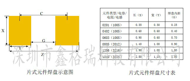
( 3 ) Chip component pad design: including resistance (exclusion), capacitance (discharge), inductance, etc.

     According to the component size and solder joint requirements, the following pad sizes can be derived:

Pad and stencil opening instructions for common components in SMT process

( 4 ) Chip component stencil opening design: including resistance (exclusion), capacitance (discharge), inductance and so on.

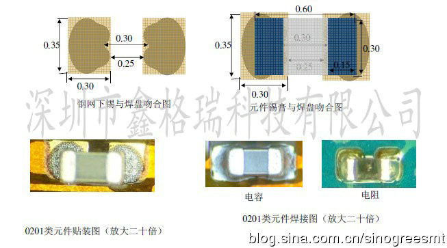
  ( 4.1 ) 0201 component steel mesh design:

         Design points: components can not be high, tombstone.

         The thickness of the steel mesh: 0.08-0.12MM , open horseshoe shape, the inner distance is kept 0.30 , and the total tin area is 95% of the pad .

Pad and stencil opening instructions for common components in SMT process

( 4.2 ) 0402 component steel mesh design:

       Design points: components can not be high, tin beads, tombstones.

      The thickness of the steel mesh: 0.10-0.15MM , the best 0.12MM , the concave anti-tin beads with 0.2 in the middle , the inner distance is kept at 0.45 , the outer three ends of the resistor are added with 0.05 , the outer three ends of the capacitor are added with 0.1 , and the total tin area is the pad. 100% to 105%. (Note: Due to the different thickness of the resistor and capacitor, the resistance is 0.3MM , the capacitance is 0.5MM, so the amount of tin is different, which is a good help for the height of the tin and the detection of the AOI optical automatic detection)

Pad and stencil opening instructions for common components in SMT process 0

( 4.3 ) 0603 type component steel mesh design:

       Design points: components to avoid tin beads, tombstones, amount of tin.

       Steel mesh thickness: 0.12-0.15MM , 0.15MM is the best. The concave anti-tin beads with 0.25 opening in the middle maintain the inner distance of 0.8 , the outer three ends of the resistor plus 0.1 , the outer three ends of the capacitor plus 0.15 , and the total tin area is 100%-110% of the pad . (Note: 0603 type components 0402 , 0201 components are together when the thickness of the stencil is limited, in order to increase the amount of tin must be added in an external way)

Pad and stencil opening instructions for common components in SMT process 1

( 4.4 ) Stencils with a size greater than 0603 ( 1.6*0.8MM )

       Design points: components to avoid tin beads, the amount of tin.

       The thickness of the steel mesh is 0.12-0.15MM , and the concave shape of the 1/3 is opened to prevent the tin beads, and the amount of tin is 90%.

Pad and stencil opening instructions for common components in SMT process 2

(5.1) SOT23 ( three-stage small crystal type ) component pad and stencil opening design

Pad and stencil opening instructions for common components in SMT process 3


(6.1) Pad and stencil opening design for airfoil components ( SOP , QFP, etc.)

The airfoil components are divided into a straight wing type and a European wing type. The straight wing type component should be inscribed in the opening of the pad stencil to prevent the component body on the solder.

Pad and stencil opening instructions for common components in SMT process 4

Pad and stencil opening instructions for common components in SMT process 5

Note: In order not to short the components between the pins, and the front end is well wetted, the stencil opening should be designed to be retracted and externally added, and should not exceed 0.25 , otherwise it will easily produce tin beads, and the thickness of the stencil should be 0.12MM. .

(6.2) Airfoil component pad and stencil opening design application

0.4MM pitch board to board connector

Pad design: pad width 0.23 (component foot width 0.18MM ), length 1.2 (component foot length 0.8MM ).

Steel mesh opening: length 1.4 , width 0.2 , steel mesh thickness: 0.12MM .

Pad and stencil opening instructions for common components in SMT process 6
(7.1) QFN type component pads and stencil opening design

The QFN ( Quad Flat No Lead ) component is a leadless component that is widely used in the high frequency field, but its soldering structure is castellated and is leadless soldered, so there is a certain amount in the SMT soldering process. Difficulty.

Pad and stencil opening instructions for common components in SMT process 7

(7.2) Combining the dimensions of the QFN components themselves with the solder joint requirements The pad and stencil opening design correspond to the following:

Key points: Do not produce tin beads, float high, short circuit, and increase the amount of solderable ends and tin.

Method: The pad design is at least 0.15-0.30MM to the solderable end of the component size (maximum of 0.30MM , otherwise the component is prone to insufficient tin height).

Stencil: Add 0.20MM on the basis of the pad , and open the hole in the middle heat-dissipating pad to prevent the component from flying high.

Pad and stencil opening instructions for common components in SMT process 8

(7.3) A typical QFN type component pad and stencil opening design

    Components: 0.4MM pitch QFN , solderable end length 0.6MM , width 0.2.

     Pad: length 0.75 , width 0.25.

     Steel mesh: length 0.95 , width 0.22 ( extended to prevent short-circuit solder balls), the middle heat-dissipating block is opened by 80% bridge to prevent false welding caused by floating height.

Pad and stencil opening instructions for common components in SMT process 9

(8.1) BGA ( Ball Grid Array ) class component size:

Pad and stencil opening instructions for common components in SMT process 0

BGA ( Ball Grid Array ) components are based on the diameter and spacing of the solder balls when designing the pads :

After soldering, the solder ball melts and forms an intermetallic compound with solder paste and copper and platinum. At this time, the diameter of the ball becomes smaller, and the solder paste during melting retracts under the action of intermolecular force and liquid tension, thereby obtaining a pad. The design with the steel mesh is as follows:

(1)       The pad design is typically 10%-20% smaller than the ball diameter .

(2)       The opening of the stencil is 10%-20% larger than the pad .

Note: except when fine pitch, this time at 100% open during 0.4pitch, generally less than 0.4 at 90% open to prevent shorting.

Pad and stencil opening instructions for common components in SMT process 8

BGA type components pay attention to problems such as voids and short circuits on the solder joints during soldering. There are many factors in the emergence of such problems, such as BGA baking, secondary reflow of PCB , etc., the length of reflow time, but should pay attention to the pad and steel mesh:

1. When designing the pad, please pay attention to avoiding the through hole as much as possible. Buried holes such as buried holes may appear on the pad.

2, the larger the pitch BGA (more than 0.5MM) of the tin can be added by thickening the amount of steel mesh or larger opening is achieved, for BGA fine pitch (less than 0.4MM) and should be reduced diameter stencil opening thickness.

Remarks: Steel mesh refers to steel mesh made by laser electropolishing technology.

      Solder paste refers to a lead-free solder paste of SnAg ( 3.5 ) Cu ( 0.5 ).

PCB refers to a fiberboard made of FR4 .

FPC refers to a flexible circuit board.
Entre em contato conosco

Author:

Mr. Kevin

Phone/WhatsApp:

+8613165553600

Produtos populares
You may also like
Related Categories

Enviar e-mail para este fornecedor

Assunto:
E-mail:
mensagem:

Your message must be betwwen 20-8000 characters

We will contact you immediately

Fill in more information so that we can get in touch with you faster

Privacy statement: Your privacy is very important to Us. Our company promises not to disclose your personal information to any external company with out your explicit permission.
enviar